

Carrier Board for Advanced Phase-Shift PWM Controller UCC3895
- Rajkumar Sharma
- 621 Views
- medium
- Tested
- SKU: EL117625
- Quote Now
- 0 Likes

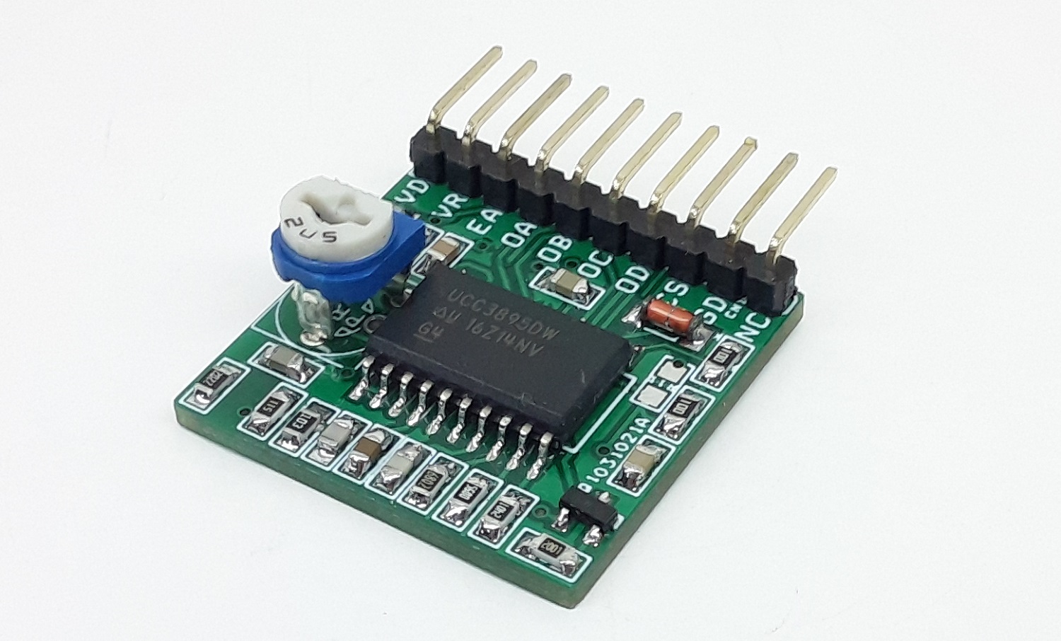
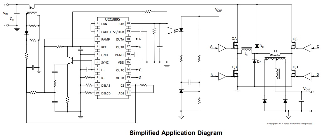
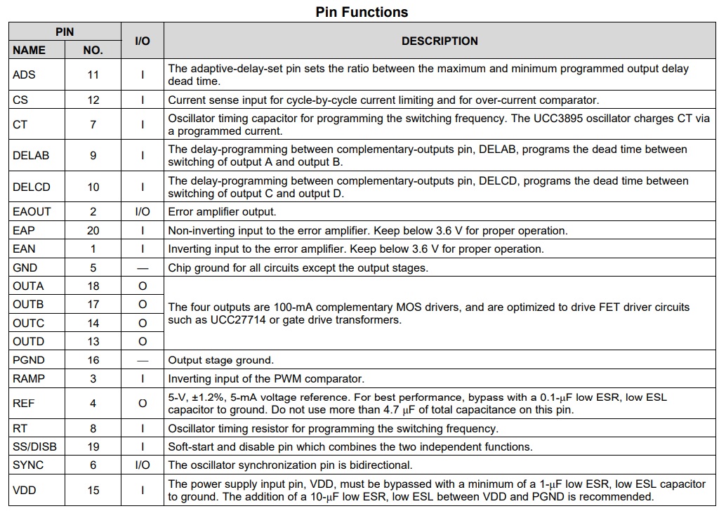
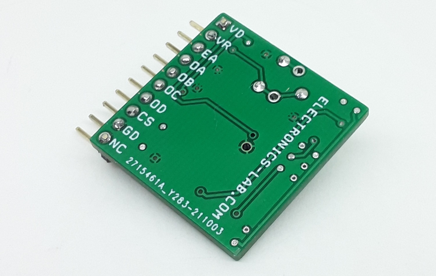
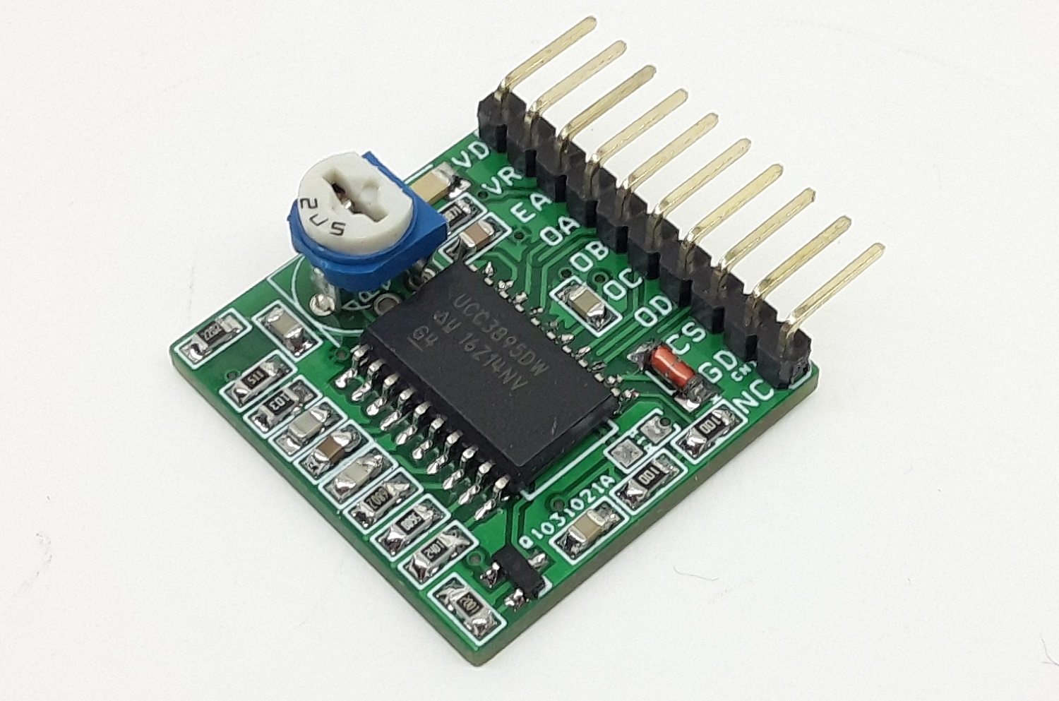
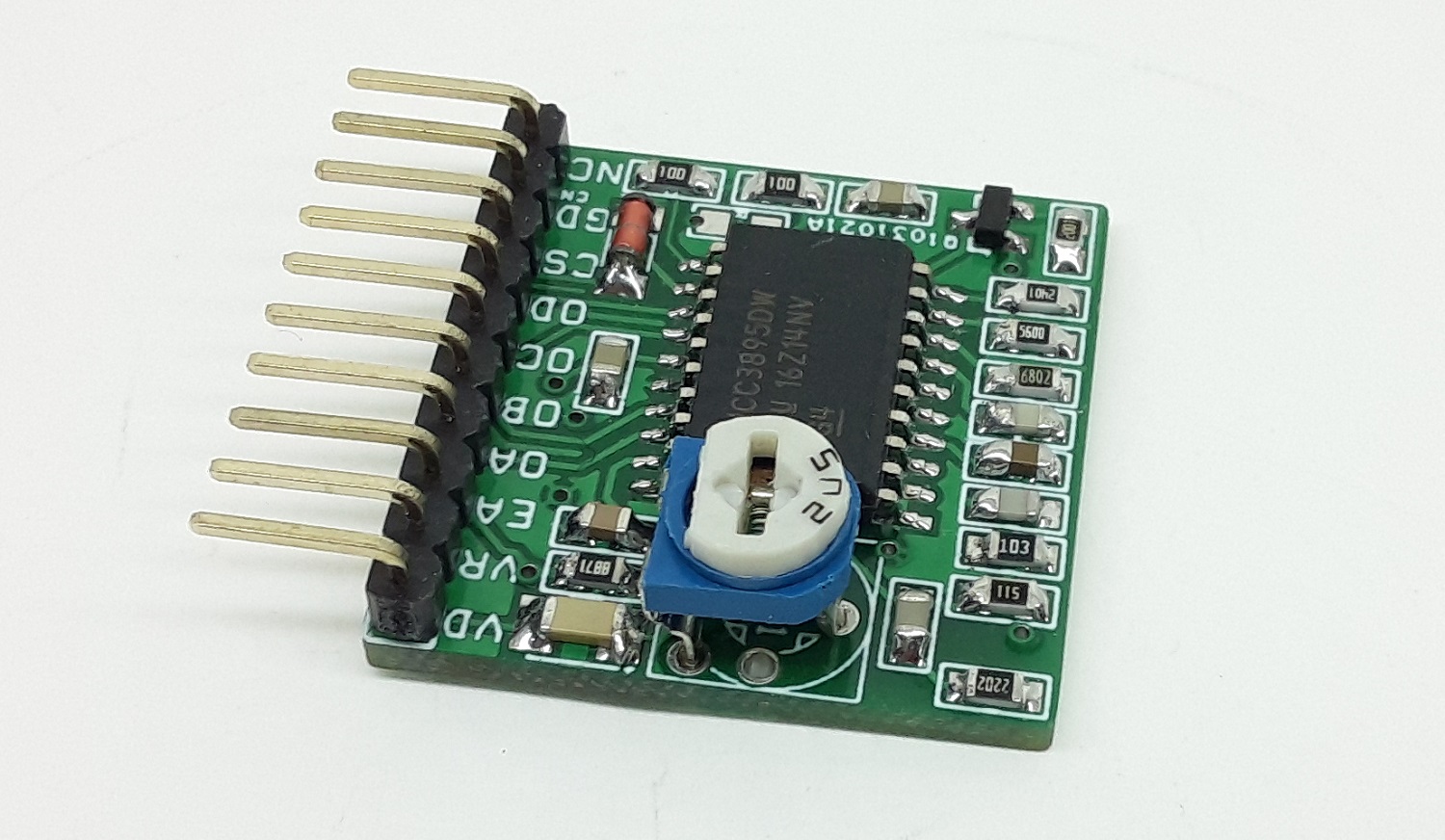
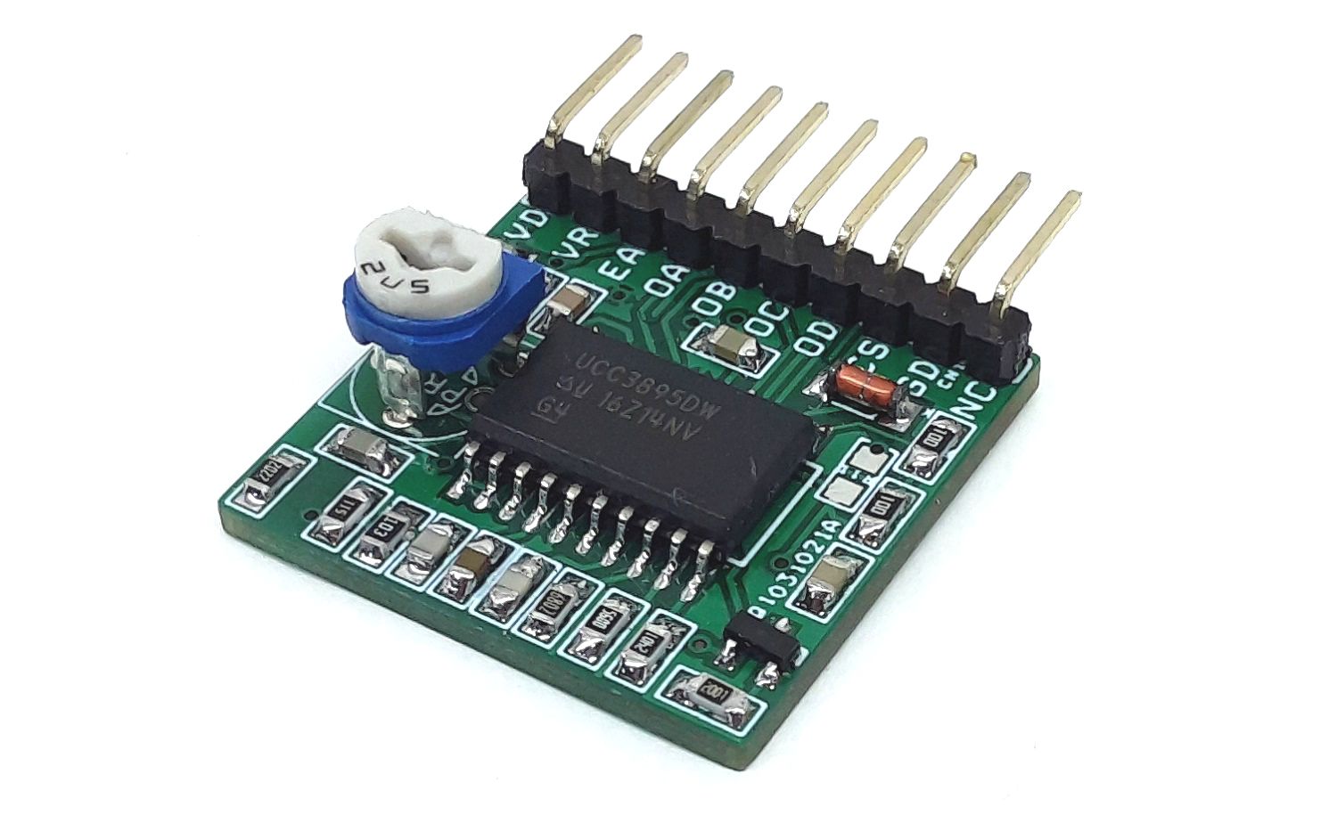
This is a Phase-Shifted Full-Bridge PWM UCC3895 carrier board that contains all of the features necessary to implement a phase-shifted full-bridge topology power converter. All inputs and outputs pins are accessible using a header connector. A highly-efficient DC-DC converter can be created using this carrier board + External H-Bridge and Transformer. Refer to the datasheet of UC3895 and schematic to configure the working frequency, current feedback, delays, etc.
The UCC3895 is a phase-shift PWM controller that implements control of a full-bridge power stage by phase-shifting the switching of one half-bridge with respect to the other. The device allows constant frequency pulse-width modulation in conjunction with resonant zero-voltage switching to provide high efficiency at high frequencies. The part is used either as a voltage-mode or current-mode controller. While the UCC3895 maintains the functionality of the UC3875/6/7/8 family and UC3879, it improves on that controller family with additional features such as enhanced control logic, adaptive delay set, and shutdown capability. Because the device is built using the BCDMOS process, it operates with dramatically less supply current than its bipolar counterparts. The UCC3895 operates with a maximum clock frequency of 1 MHz.
Note: This is a carrier board for UCC3895 phase-shift chip, refer to the datasheet of UCC3895 IC to learn more about setting up the delay, current sense, duty cycle, frequency.
Features
- Operating Power-Supply 10V to 16.5V DC
- Default Frequency 195Khz
- Programmable-output turn-on delay
- Adaptive delay set
- Bidirectional oscillator synchronization
- Voltage-mode, peak current-mode, or average
- current-mode control
- Programmable soft start, soft stop, and chip
- disable via a single pin
- 0% to 100% duty-cycle control
- 7-MHz error amplifier
- Operation up to 1 MHz
- Typical 5-mA operating current at 500 kHz
- Very low 150-μA current during UVLO
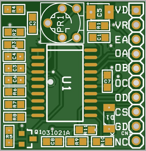
- PCB dimensions: 24.40 x 26.04 mm
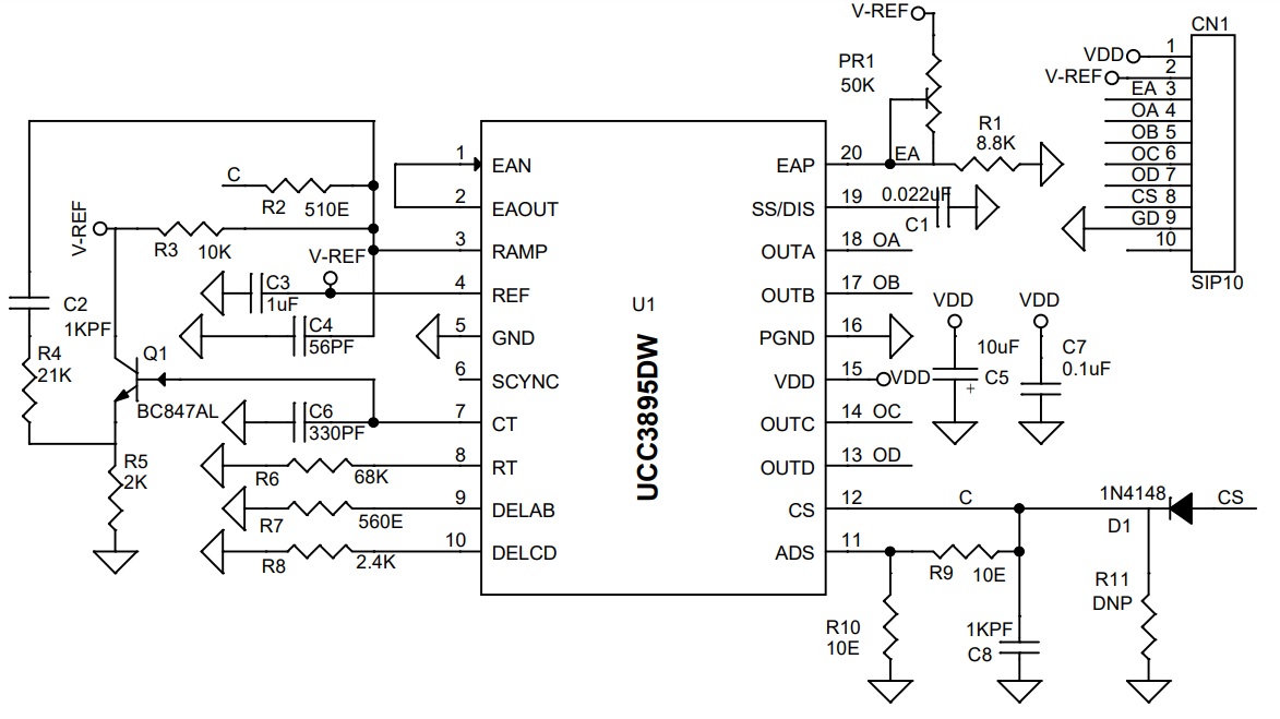
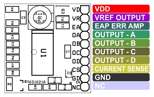
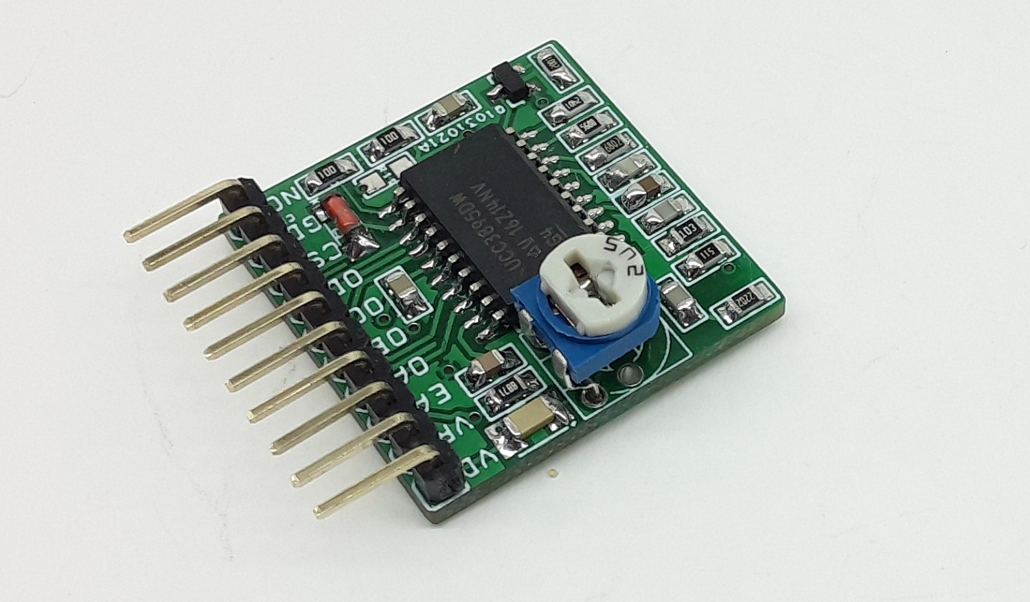
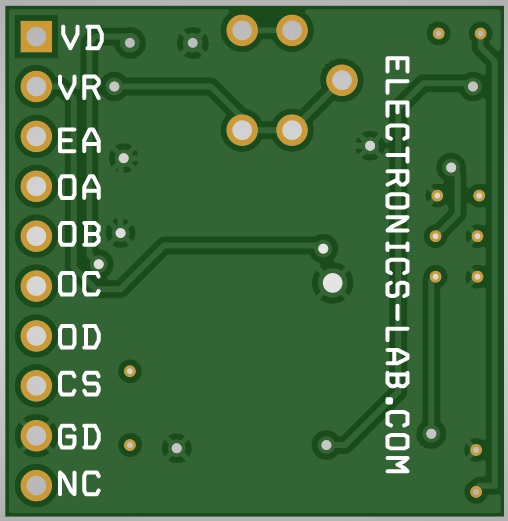
Connector CN1 Pinout
- Pin 1 VDD 10V to 16.5V DC
- Pin 2 VREF Output 5V DC
- Pin 3 Error Amplifier (EA)
- Pin 4 Output A
- Pin 5 Output B
- Pin 6 Output C
- Pin 7 Output D
- Pin 8 Current Sense In
- Pin 9 GND
- Pin 10 Not Connected ( NC)
Schematic
Application Diagram
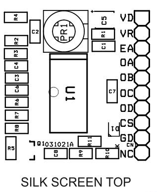
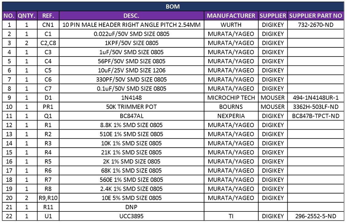
Parts List
| NO. | QNTY. | REF. | DESC. | MANUFACTURER | SUPPLIER | PART NO |
|---|---|---|---|---|---|---|
| 1 | 1 | CN1 | 10 PIN MALE HEADER RIGHT ANGLE PITCH 2.54MM | WURTH | DIGIKEY | 732-2670-ND |
| 2 | 1 | C1 | 0.022uF/50V SMD SIZE 0805 | MURATA/YAGEO | DIGIKEY | |
| 3 | 2 | C2,C8 | 1KPF/50V SIZE 0805 | MURATA/YAGEO | DIGIKEY | |
| 4 | 1 | C3 | 1uF/50V SMD SIZE 0805 | MURATA/YAGEO | DIGIKEY | |
| 5 | 1 | C4 | 56PF/50V SMD SIZE 0805 | MURATA/YAGEO | DIGIKEY | |
| 6 | 1 | C5 | 10uF/25V SMD SIZE 1206 | MURATA/YAGEO | DIGIKEY | |
| 7 | 1 | C6 | 330PF/50V SMD SIZE 0805 | MURATA/YAGEO | DIGIKEY | |
| 8 | 1 | C7 | 0.1uF/50V SMD SIZE 0805 | MURATA/YAGEO | DIGIKEY | |
| 9 | 1 | D1 | 1N4148 | MICROCHIP TECH | MOUSER | 494-1N4148UR-1 |
| 10 | 1 | PR1 | 50K TRIMMER POT | BOURNS | MOUSER | 3362H-503LF-ND |
| 11 | 1 | Q1 | BC847AL | NEXPERIA | DIGIKEY | BC847B-TPCT-ND |
| 12 | 1 | R1 | 8.8K 1% SMD SIZE 0805 | MURATA/YAGEO | DIGIKEY | |
| 13 | 1 | R2 | 510E 1% SMD SIZE 0805 | MURATA/YAGEO | DIGIKEY | |
| 14 | 1 | R3 | 10K 1% SMD SIZE 0805 | MURATA/YAGEO | DIGIKEY | |
| 15 | 1 | R4 | 21K 1% SMD SIZE 0805 | MURATA/YAGEO | DIGIKEY | |
| 16 | 1 | R5 | 2K 1% SMD SIZE 0805 | MURATA/YAGEO | DIGIKEY | |
| 17 | 1 | R6 | 68K 1% SMD SIZE 0805 | MURATA/YAGEO | DIGIKEY | |
| 18 | 1 | R7 | 560E 1% SMD SIZE 0805 | MURATA/YAGEO | DIGIKEY | |
| 19 | 1 | R8 | 2.4K 1% SMD SIZE 0805 | MURATA/YAGEO | DIGIKEY | |
| 20 | 2 | R9,R10 | 10E 5% SMD SIZE 0805 | MURATA/YAGEO | DIGIKEY | |
| 21 | 1 | R11 | DNP | |||
| 22 | 1 | U1 | UCC3895 | TI | DIGIKEY | 296-2552-5-ND |
Connections
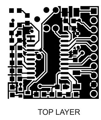
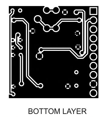
Gerber View
UCC3895 Pin Functions
Photos
Video
UCC3895 Datasheet
Please follow and like us:
PCB


Subscribe
Login
0 Comments


 – Boost Power – Factor Correction (PFC) Controller")
